- 您现在的位置:买卖IC网 > Sheet目录3753 > ATMEGA169P-16MCHR (Atmel)MCU AVR 16KB FLASH 16MHZ 64-VQFN
PIC16F946
DS41265A-page 246
Preliminary
2005 Microchip Technology Inc.
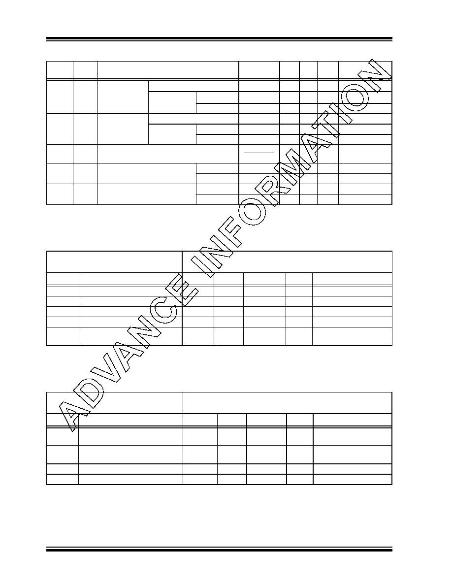
TABLE 19-8:
CAPTURE/COMPARE/PWM REQUIREMENTS
TABLE 19-9:
COMPARATOR SPECIFICATIONS
TABLE 19-10: COMPARATOR VOLTAGE REFERENCE SPECIFICATIONS
Param.
No.
Sym
Characteristic
Min
Typ Max Units Conditions
50*
TCCL
CCP1
input low time
No Prescaler
0.5TCY + 5
—
ns
With Prescaler
3.0-5.5V
10
—
ns
2.0-5.5V
20
—
ns
51*
TCCH
CCP1
input high time
No Prescaler
0.5TCY + 5
—
ns
With Prescaler
3.0-5.5V
10
—
ns
2.0-5.5V
20
—
ns
52*
TCCP
CCP1 input period
3TCY + 40
N
—
ns
N = prescale
value (1,4 or 16)
53*
TCCR
CCP1 output fall time
3.0-5.5V
—
10
25
ns
2.0-5.5V
—
25
50
ns
54*
TCCF
CCP1 output fall time
3.0-5.5V
—
10
25
ns
2.0-5.5V
—
25
45
ns
*
These parameters are characterized but not tested.
Data in “Typ” column is at 5V, 25°C unless otherwise stated. Parameters are for design guidance only and
are not tested.
Comparator Specifications
Standard Operating Conditions (unless otherwise stated)
Operating temperature
-40°C
≤ TA ≤ +125°C
Sym
Characteristics
Min
Typ
Max
Units
Comments
VOS
Input Offset Voltage
—
±5.0
±10
mV
VCM
Input Common Mode Voltage
0
—
VDD – 1.5
V
CMRR
Common Mode Rejection Ratio
+55*
—
db
TRT
Response Time(1)
—
150
400*
ns
TMC2COV
Comparator Mode Change to
Output Valid
——
10*
μs
*
These parameters are characterized but not tested.
Note 1:
Response time measured with one comparator input at (VDD – 1.5)/2 while the other input transitions from
VSS to VDD – 1.5V.
Voltage Reference Specifications
Standard Operating Conditions (unless otherwise stated)
Operating temperature
-40°C
≤ TA ≤ +125°C
Sym.
Characteristics
Min
Typ
Max
Units
Comments
Resolution
—
VDD/24*
VDD/32
—
LSb
Low Range (VRR = 1)
High Range (VRR = 0)
Absolute Accuracy
—
±1/4*
±1/2*
LSb
Low Range (VRR = 1)
High Range (VRR = 0)
Unit Resistor Value (R)
—
2K*
—
Ω
Settling Time(1)
——
10*
μs
*
These parameters are characterized but not tested.
Note 1:
Settling time measured while VRR = 1 and VR<3:0> transitions from ‘0000’ to ‘1111’.
发布紧急采购,3分钟左右您将得到回复。
相关PDF资料
2-1546217-0
TERM BLK RCPT 20POS SIDE 5.08MM
1-1546217-9
TERM BLK RCPT 19POS SIDE 5.08MM
1-1546217-8
TERM BLK RCPT 18POS SIDE 5.08MM
1-1546217-7
TERM BLK RCPT 17POS SIDE 5.08MM
1-1546217-6
TERM BLK RCPT 16POS SIDE 5.08MM
1-1546217-5
TERM BLK RCPT 15POS SIDE 5.08MM
1-1546217-4
TERM BLK RCPT 14POS SIDE 5.08MM
1-1546217-3
TERM BLK RCPT 13POS SIDE 5.08MM
相关代理商/技术参数
ATMEGA169P-16MCU
功能描述:8位微控制器 -MCU AVR 16KB, 512B EE 16MHz 1KB SRAM, 5V
RoHS:否 制造商:Silicon Labs 核心:8051 处理器系列:C8051F39x 数据总线宽度:8 bit 最大时钟频率:50 MHz 程序存储器大小:16 KB 数据 RAM 大小:1 KB 片上 ADC:Yes 工作电源电压:1.8 V to 3.6 V 工作温度范围:- 40 C to + 105 C 封装 / 箱体:QFN-20 安装风格:SMD/SMT
ATMEGA169P-16MU
功能描述:8位微控制器 -MCU AVR 16K FLASH 512B EE 1K SRAM LCD ADC RoHS:否 制造商:Silicon Labs 核心:8051 处理器系列:C8051F39x 数据总线宽度:8 bit 最大时钟频率:50 MHz 程序存储器大小:16 KB 数据 RAM 大小:1 KB 片上 ADC:Yes 工作电源电压:1.8 V to 3.6 V 工作温度范围:- 40 C to + 105 C 封装 / 箱体:QFN-20 安装风格:SMD/SMT
ATMEGA169P-16MU SL383
制造商:Atmel Corporation 功能描述:MCU 8BIT ATMEGA RISC 16KB FLASH 3.3V/5V 64PIN MLF - Tape and Reel
ATMEGA169P-16MUR
功能描述:8位微控制器 -MCU AVR LCD 16KB FLSH EE 512B 1KB SRAM-16MHZ RoHS:否 制造商:Silicon Labs 核心:8051 处理器系列:C8051F39x 数据总线宽度:8 bit 最大时钟频率:50 MHz 程序存储器大小:16 KB 数据 RAM 大小:1 KB 片上 ADC:Yes 工作电源电压:1.8 V to 3.6 V 工作温度范围:- 40 C to + 105 C 封装 / 箱体:QFN-20 安装风格:SMD/SMT
ATMEGA169P-8AU
制造商:ATMEL 制造商全称:ATMEL Corporation 功能描述:Microcontroller with 16K Bytes In-System Programmable Flash
ATMEGA169P-8MU
制造商:ATMEL 制造商全称:ATMEL Corporation 功能描述:Microcontroller with 16K Bytes In-System Programmable Flash
ATMEGA169PA
制造商:ATMEL 制造商全称:ATMEL Corporation 功能描述:8-bit Microcontroller with 16K Bytes In-System Programmable Flash
ATMEGA169PA_1
制造商:ATMEL 制造商全称:ATMEL Corporation 功能描述:High Endurance Non-volatile Memory segments